Seller Note “Was given to me by a friend and has been laying around in a draw safely for a while now has not been tested and don’t know if it is still working. have no way of testing it either” – sounds like a typical Ebay seller fake cover story…
Summary
- This card has a 12v short on the PCI (of course a friend gave it to them, nice gift of a card that is clearly broken!)
- Sadly, I strongly suspect that the 12v reached the core after injecting 1v.
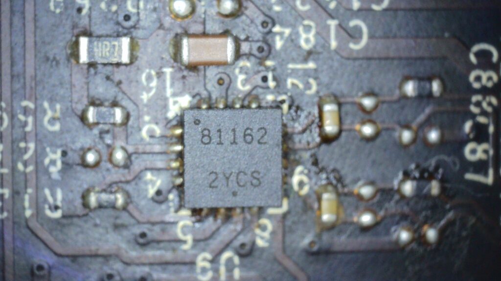
- I have located the shorted VCore dual MOSFET (U4536) using an ESR meter. This inductor showed less than 0.9 Ohm, all others 1.04 Ohms. This dual MOSFET is also featuring a solder bubble.
- There is another problem, fuse F1 seems somewhat vapourised!
- Overall, due to that short, I would fully expect this card to be spare parts, as the core probably saw 12v at some point. However, I will still go ahead to try and resolve the short, assuming the dual MOSFET can be easily removed.
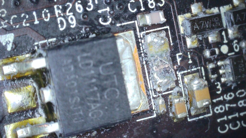
Used a preheater and 450 degrees C hot air and the dual MOSFET came off nice and easy.
Amazing! Not sure how, but I have normal voltages and a BIOS picture! 🙂
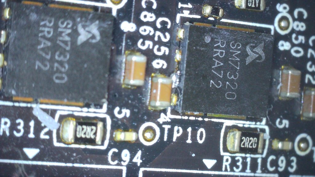
That dual MOSFET is http://www.sinopowersemi.com/temp/SM7320ESQG_datasheet.pdf
Now there’s a chance this is fixable, I should next
- Check the VRM is stable (oscilloscope)
- Replace the cooler and check if I can get to windows and load drivers (GPU might still be compromised)
- Check readings to see if the PWM and driver resistances for that phase seem normal
- Find that fuse
- order parts
This could be 1206L035YR or similar. 350mv resettable fuse size 01206.
The doublers and drivers on this card look somewhat corroded, might be an idea to order some new ones if they are cheap. They might actually be OK, as I measured the same resistances across the gates of the MOSFETs. They are likely not! As for the record, I foolishly tried replacing U4536 and it blew again!
Update 28/08/2022 – Deep dive on phases 1 and 4.
Whilst phase 1 (U4536) was the dual MOSFET that blew, the way the VRM is designed (with PWM signal doublers, double drivers and double MOSFETs) means phase 4 might also have an issue if say the doubler or driver also has a fault. From top to bottom of the card (where the PCI slot is), the phases are laid out like this:
| Phase | PWM SIgnal Doubler | Double MOSFET Driver | Double MOSFET |
|---|---|---|---|
| 3 | U12 | U15 | U4538 |
| 6 | U4539 | ||
| 2 | U13 | U16 | U4540 |
| 5 | U4541 | ||
| 4 | U9 | U17 | U4536 (blown) |
| 1 | U4537 |
I have some replacement drivers and doublers now, so I am hopefully in a better position to try and repair the faulty phase. Experience has taught me to not simply replace the missing dual MOSFET, power up and hope for the best. I want to understand what the underlying issue is.
- All high and low gate resistances appear consistent.
- I still don’t know why the 5v fuse is partially vapourised (the 5V resistance appears normal or not shorted at least), the melted fuse could be a clue to something drawing too much current on the 5V rail. The doublers take 5V as VCC, so the doubler for phases 1 and 2 (U9) is a suspect and should be investigated.
- As the card stands (with U4536 removed) and no shorts on the DRMOS gates, it should be safe (always some risk) to power on the card without any load and check the waveforms on the gates for phases 1 and 2.
- That melted 5V fuse should also be replaced.
Results
- 5.17V from the 5V regulator, but only ~3V on the far end of that melted fuse! I guess it works enough to power the double drivers and whatever else needs 5V, but that voltage drop cannot be healthy.
- Waveforms for phases 3,6,2,5 all look the same (good). Phase 4 is of course flat (no double MOSFET to drive it). However, phase 1 doesn’t look like the good phases (fewer pulses about 3 vs about 7 on the healthy phases). Unless there is something else on the 5V rail that is faulty that I haven’t yet detected, I have to suspect that doubler. Could be worth injecting 5V and seeing if there is any heat? I couldn’t see any shorted inputs when I checked. Injecting 3.5V draws almost no current, so probably no shorts on the 5V rail. The fact that the phase 1 waveform looks compromised, makes me further suspect the doubler. Should double check all 3 PWM signals are identical.
Given these results. I think the next steps should be:
TLDR; measure what I can, replace the fuse, doubler and driver!
- Check gate pads 1 and 8 of U4536 and compare to a healthy phase, mainly out of interest to see
- Check the 3 PWM signals are the same.
- Find a replacement for that fuse. I haven’t got one and removing the remains could also take more effort.
- Replace the doubler.
- Test phase 1 waveform, see if it now matches that of the healthy phases. Again, just for curiosity really.
- If not, also replace the double driver (probably worth doing anyway. Really, think this is a good idea anyway, as there are some traces of corrosion.
- When all phases look good, try replacing U4536.
Results
- Measured gate pads of U4536 (phase 4) and they are identical to those of it’s related phase 1 i.e. the waveform consists of 3 pulses rather than the 7 on the healthy phases.
- Replaced 5V fuse F1 with a donor card fuse, the 5V rail measures just under 5V (~4.85V)
Damn it! I got distracted and removed and cleaned the double and driver for healthy phases 3 and 6! Remarkably they crad started and has a picture. The chips actually looked quite dirty, so hopefully I’ll get away with it and can replace these too. At least it’s easier to measure without doubler U12 in place:
- measuring Doubler U12 pin
- 4 (EN) – 2.33V
- 5 (RDY) – 4.5+
- 6 (DRVON) – 4.95V
- 7 (PWM1) Oscilloscope
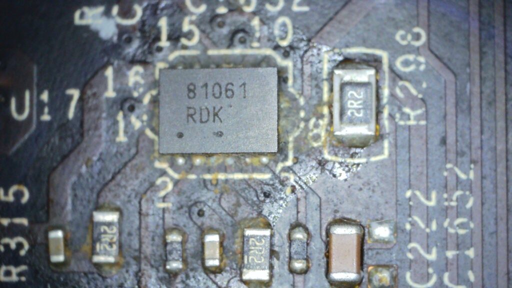
- Have removed both doubler U7 and double driver U17
TODO Add pictures of replacing the 5V fuse.
TODO Add details of blown MOSFET
Luckily, whilst there is PCB damage under phase 6, it could be worse and the card still managed a BIOS picture even on only two phases.
LG should be ~33K
HG should be ~7.8K
phase 3 – LG OL, HG 9.36K
phase 6 – LG and HG are OL!
I must have fitted the double driver wrong and paid the price. This was avoidable, as I was rushing and should never have tested the card without first checking the gate resistances that are clearly wrong! I am not yet sure what exactly is wrong though. I will continue to investigate.
phase 4 –
phase 1 –
Another problem that I had foolishly overlooked due to phase 1 producing a wave form, was that the high gate resistance was ~10K vs the 7.88K it should be.
TODO add pic
I removed replaced 0603 1 Ohm resistor R319, but it wasn’t the problem as it measured 1.1 Ohms. Therefore this adds to the phase 1 double MOSFET being faulty, I will replace this too. Well, this is puzzling me? Even the new high-side gate for phase 1 measures 10K rather than 7. I am starting to suspect that either:
1) I am not fitting the driver correctly and pad 12 is not connected?
2) There is something wrong with the trace or pad 12 itself? A clue might be that phase 3 currently has no driver or MOSFET present, and it’s high gate measures 10K…
TODO Add photo of discovery that the high gate resistance drops from 10K to 7.8K only when the driver is properly soldered.
There seems to be either a broken pad or trace under the driver. I am going to take a break, as I don’t seem to be able to locate it exactly..